[email protected]
 Monday to Friday 8 a.m.- 5 p.m.
Call Us +86-13968655659
[email protected] Monday to Friday 8 a.m.- 5 p.m.Industry News
 2025.06.20
 Industry News
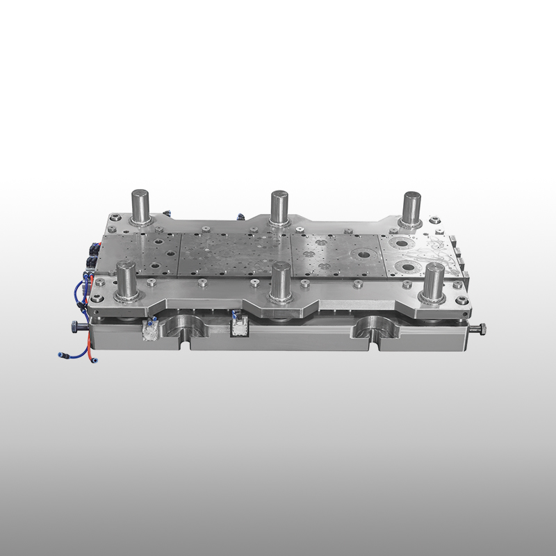
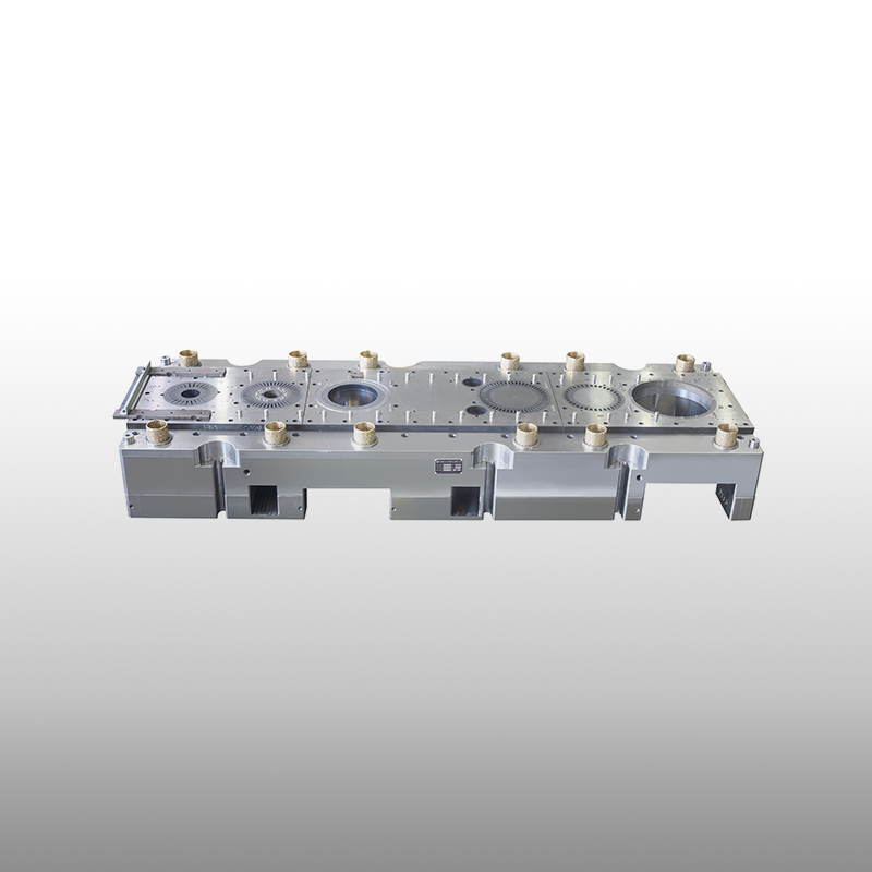
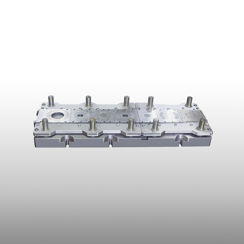
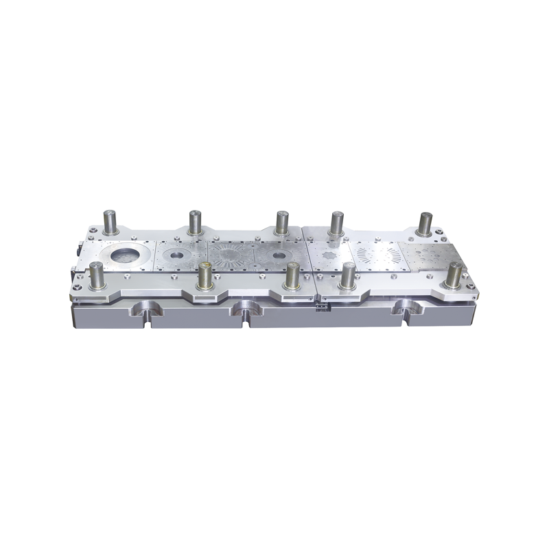
The electronics industry is known for its fast-paced innovation, high-volume production, and demand for dimensional accuracy. Among the many manufacturing processes that support this industry, Stamping Die Design plays a vital role in enabling the production of consistent, complex, and miniaturized components. Precision Stamping Die Design ensures that the metal parts used in electronic devices meet performance, tolerance, and cost expectations.
The Importance of Stamping Die Design in Electronics Manufacturing
Stamping Die Design is the process of creating the tools that shape, cut, and form metal sheets into specific components. In electronics, these components include connector pins, EMI shielding, frames, contacts, terminals, brackets, and housings. The increasing complexity of modern electronics demands Stamping Die Design solutions that can accommodate tighter tolerances and intricate geometries without compromising production efficiency.
Precision in Stamping Die Design ensures that each part fits seamlessly into final assemblies, whether it’s a smartphone, laptop, or control module. Consistency in part dimensions helps reduce rejection rates and minimizes the need for secondary machining or adjustment, which is crucial for mass production.
Material Utilization and Miniaturization
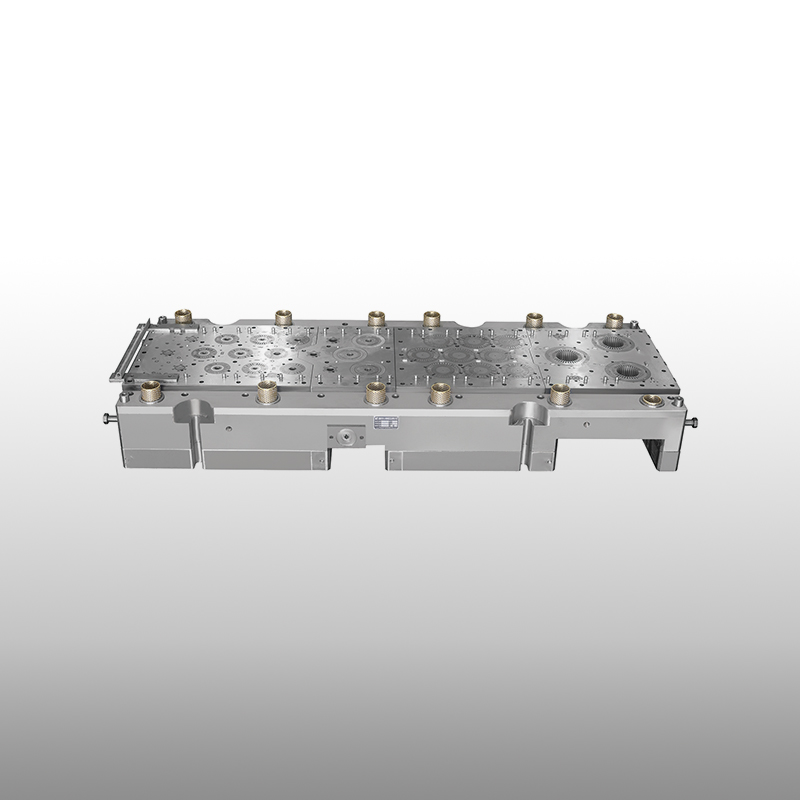
As the electronics industry continues to move toward miniaturization, Stamping Die Design must evolve to handle very thin materials such as copper alloys, stainless steel, and nickel-based materials. The design must account for material springback, burr formation, and edge quality. Efficient Stamping Die Design reduces material waste and enhances part precision, which is critical in high-volume electronics production where thousands or even millions of parts are manufactured daily.
Progressive Stamping Die Design is often employed in electronics applications to allow multiple operations, such as piercing, bending, coining, and forming, to be completed in a single pass. This not only increases efficiency but also reduces material handling and alignment errors.
Supporting High-Speed Production
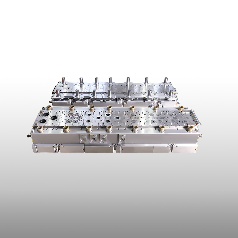
One of the key advantages of refined Stamping Die Design is its compatibility with high-speed stamping presses. In electronics manufacturing, production lines are often required to operate at several hundred strokes per minute. The design of the die must ensure smooth feeding, precise alignment, and reliable part ejection to prevent damage or downtime.
High-speed operations place stress on both the tooling and the materials. Therefore, Stamping Die Design must consider tool steel selection, lubrication channels, and wear resistance to ensure consistent operation over long production runs. This attention to detail in Stamping Die Design translates to fewer tool changes, less maintenance, and more stable production cycles.
Tolerance and Repeatability
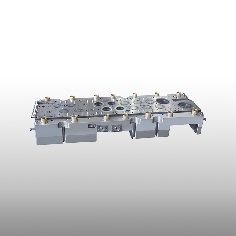
In electronic components, even slight dimensional deviations can to signal loss, mechanical failure, or assembly issues. This is why Stamping Die Design is so critical in maintaining repeatability. A well-designed stamping die can hold tolerances in the micron range, which is essential for parts that must fit into precisely engineered circuit boards or interfaces.
The integration of 3D CAD and simulation software into the Stamping Die Design process helps identify potential issues such as material thinning, wrinkling, or cracking before the die is manufactured. By validating designs in a digital environment, engineers can optimize the geometry for better performance, to higher first-pass yields and fewer prototype revisions.
Customization and Rapid Development
The electronics industry frequently introduces new product designs with shorter life cycles. As a result, Stamping Die Design must be agile enough to support quick development of new tooling. Modular and standardized die components are often used to accelerate design changes. Custom Stamping Die Design allows manufacturers to meet the specific dimensional and performance requirements of new electronic devices while keeping development times short.
Cost Efficiency Over Time
Although initial investment in precision Stamping Die Design can be significant, the long-term benefits in terms of efficiency, consistency, and scalability make it a cost-effective solution. High-quality Stamping Die Design contributes to lower scrap rates, faster production speeds, and fewer operational interruptions, which all contribute to reduced total cost of ownership.
In addition, many electronics manufacturers are moving toward in-house or localized Stamping Die Design to gain better control over supply chain timelines and design confidentiality. This internal capability enables faster revisions, better integration with production, and more effective quality control.
The electronics industry relies heavily on the accuracy, speed, and efficiency that Stamping Die Design brings to the production floor. From tiny connectors to intricate shielding components, every part demands precision engineering supported by optimized Stamping Die Design. As electronic products become smaller and more complex, the importance of advanced Stamping Die Design continues to grow. By investing in high-quality, adaptable tooling solutions, electronics manufacturers can meet evolving market needs with confidence and consistency.
Recommended Products

Sale Precision Stamping Mold Company

 English
 Español
 русский